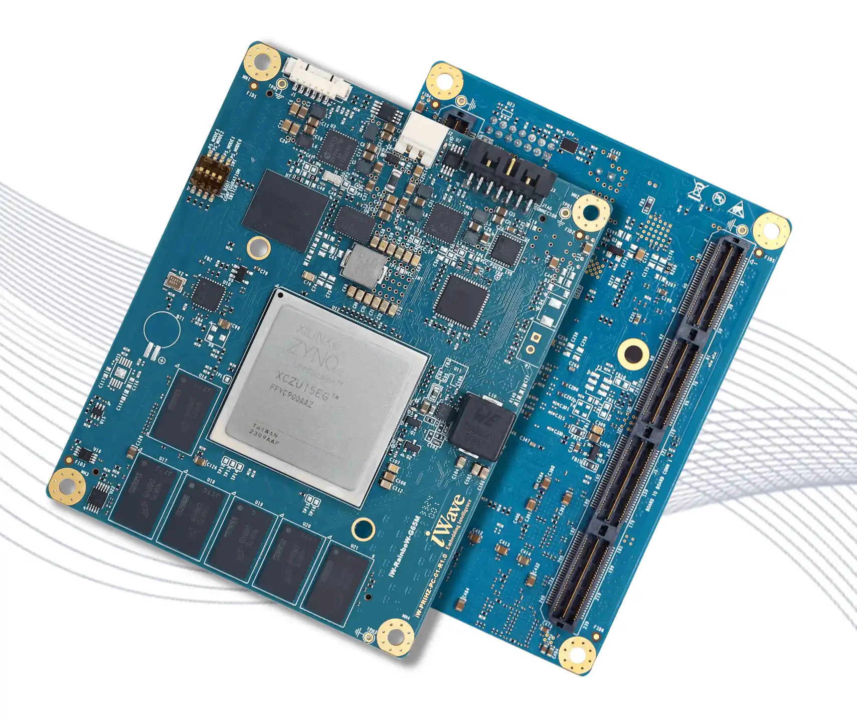
ZynqTM UltraScale+TM ZU15/ZU9/ZU6 System on Module

ZynqTM UltraScale+TM ZU15/ZU9/ZU6 System on Module

    • Zynq™ UltraScale+™ MPSoC family with FFVC900 package
    • Compatible with ZU15/ZU9/ZU6 EG/CG devices
    • 4GB DDR4 for PS with ECC, 2GB DDR4 for PL & 32GB eMMC Flash
    • 16 Channels GTH Transceivers up to 16.3Gbps
    • 4 Channels GTR Transceivers up to 6Gbps
    • 48 LVDS Pairs/ 96 SE IOs, 46 SE FPGA IOs
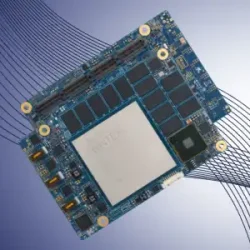
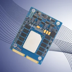
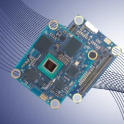
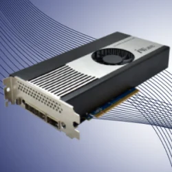
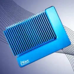
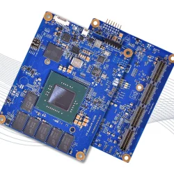
  • Zynq UltraScale ZU15ZU9ZU6 SoM Thumbnail iWave Global
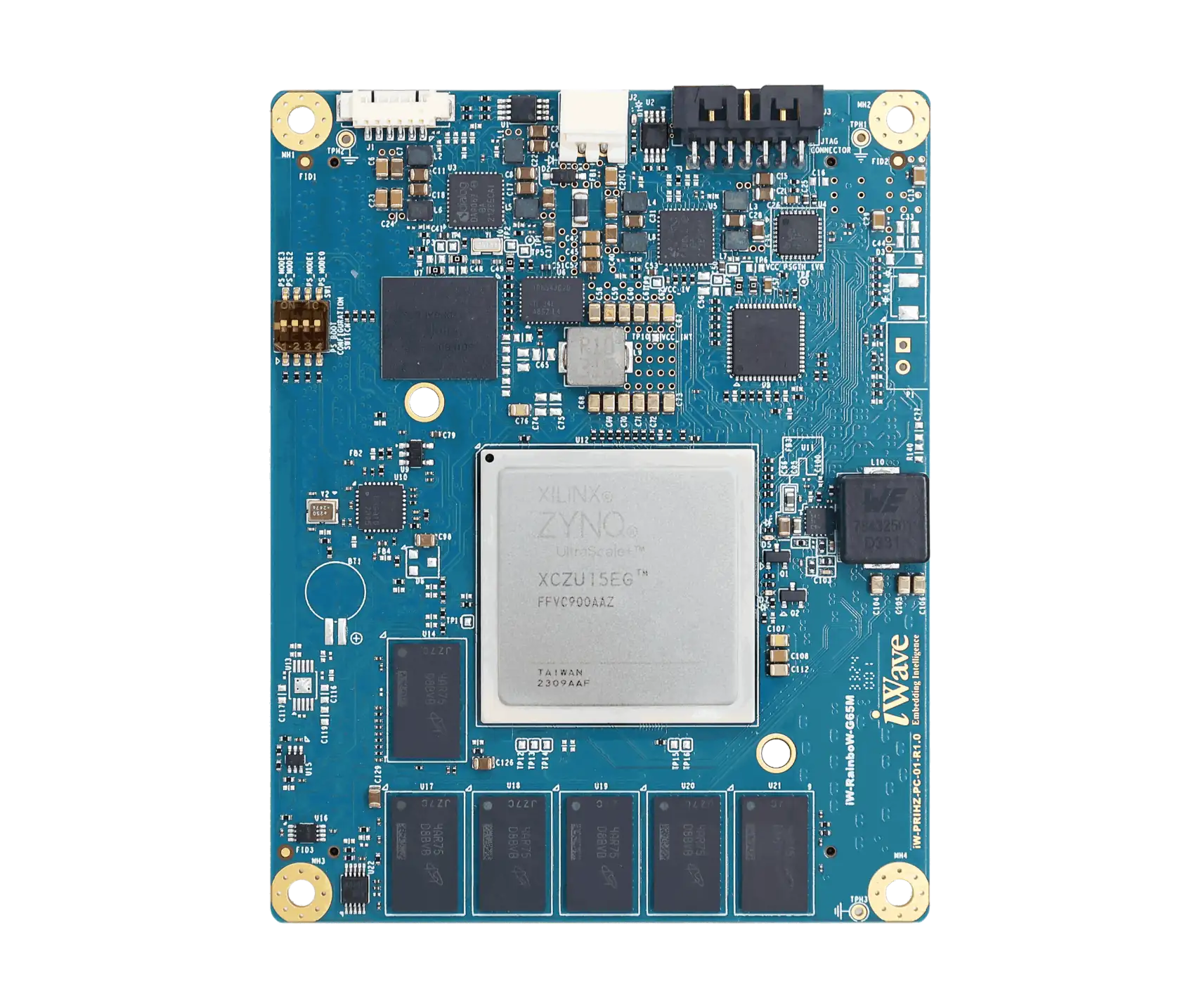
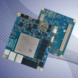
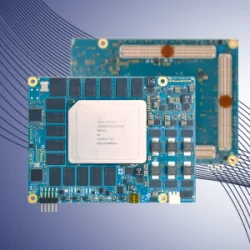
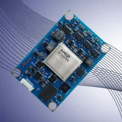
  • Zynq UltraScale ZU15ZU9ZU6 SoM Top View iWave Global
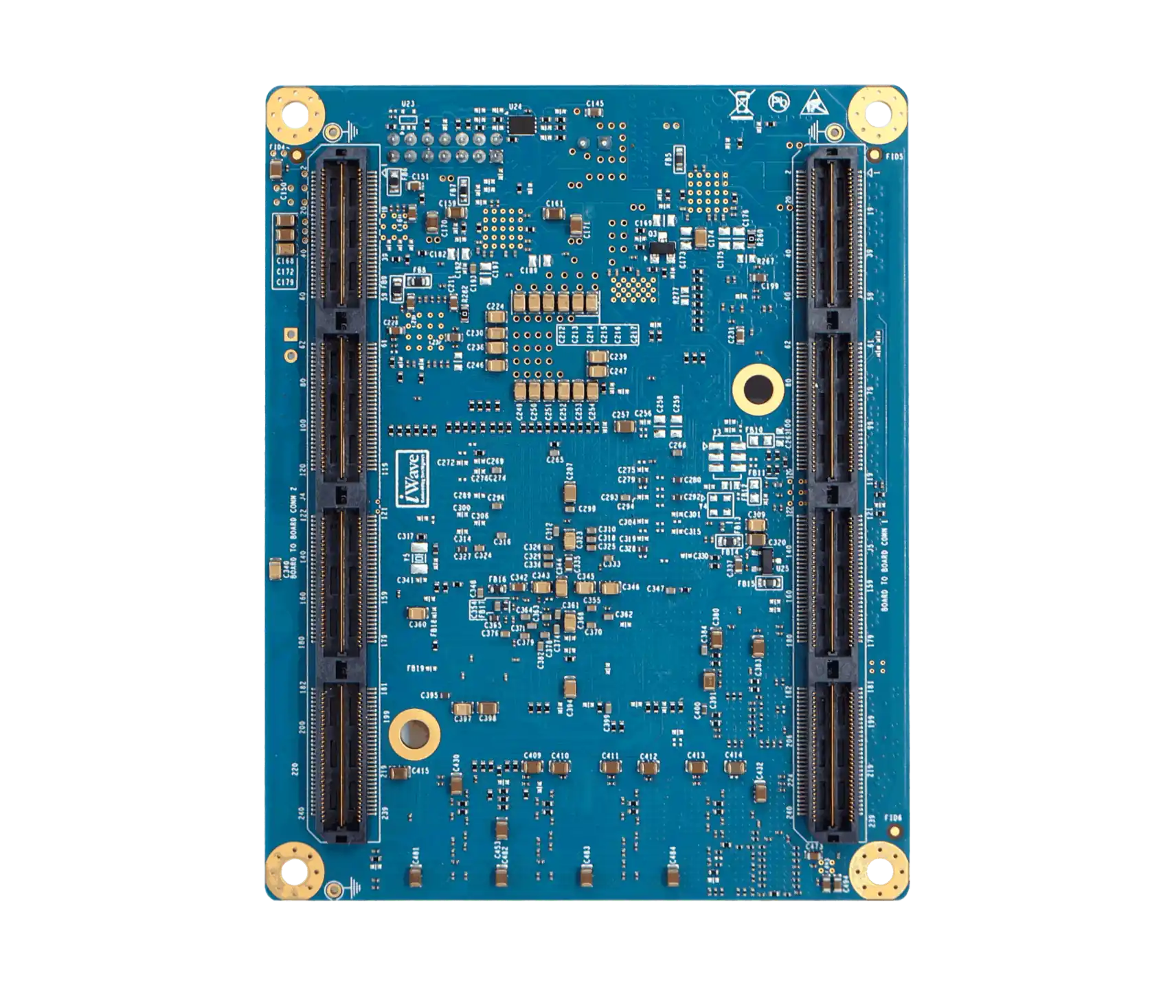
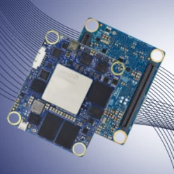
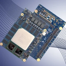
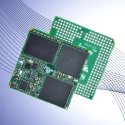
  • Zynq UltraScale ZU15ZU9ZU6 SoM Bottom View iWave Global

Documents

  • Specification
  • Development Kit
  • Custom Design
FeaturesDetails
ZU15EG ZU9/6 EG/CG - ZynqTM Ultrascale+TM MPSoC (FFVC900)

Processing System (PS/Processor)

  • Quad-core ARM Cortex-A53 MPCore @1.5GHz
  • Dual-core ARM Cortex-R5 MPCore @600MHz
  • Arm Mali-400MP2 GPU

Programming Logic (PL/FPGA)

  • Up to 747K Logic cells & 341K LUTs
  • High Speed GTH Transceivers x 16 (Up to 16.3Gb/s)
RAM Memory

PS: 64bit, 4GB DDR4 RAM with ECC (Expandable up to 8GB)
PL/FPGA: 16bit, 1GB DDR4 RAM (Expandable up to 2GB)

On Board Flash

8GB eMMC Flash for boot & storage (expandable up to 128GB)
EEPROM (4Kbit)

Other Interfaces

Gigabit Ethernet PHY Transceiver (PTP supported)
USB2.0 PHY Transceiver
6 Output programable clock synthesizer

240pin High-Speed Board to Board Connector 1 Interfaces

From PS Block

  • PS GTR Transceiver Lanes x 2 (Up to 6.0Gb/s)
  • GEM3 RGMII Interface or ULPI Interface x 1
  • CAN interface x 2

From PL Block

  • High Speed GTH Transceiver Lanes x 12 (Up to 16.3Gbps)
  • HD Bank IOs – Up to 23LVDS/46 Single Ended IO’s
  • ADC Input pins- Up to 20 Differential/Single Ended from HD Banks
240pin High-Speed Board to Board Connector 2 Interfaces

From PS Block

  • PS GTR Transceiver Lanes x 2 (Up to 6.0Gb/s)
  • Gigabit Ethernet x 1 Port (through On-SOM Gigabit Ethernet PHY)
  • 0 OTG x 1 Port (through On-SOM USB2.0 transceiver)
  • SD (4bit) x 1
  • Debug UART & Data UART x 1
  • SPI x 1
  • I2C x 2 Port
  • JTAG x 1

From PL Block

  • High Speed GTH Transceiver Lanes x 4 (Up to 16.3Gbps)
  • HP Bank IOs – 48 LVDS/96 Single Ended IO’s
  • ADC Input pins – Up to 32 Differential/Single Ended from HP Banks
General Features

Power Input: 5VDC +/- 5% input from B2B Connector2
Form Factor: 95mm X 75mm(OREN)
BSP Support: Linux
Operating Temperature: -40°C to +85°C (Industrial)
Environment Specification: REACH & RoHS3 Compliant
Compliance: CE*

*Under Progress

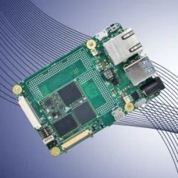
  • 10G Ethernet through SFP+ Connector
  • 3G SDI Video IN through HD BNC Connector
  • 3G SDI Video OUT through HD BNC Connector
  • Dual FMC High Pin Count (HPC) Connector
  • DP1.2a Display Port Connector
  • PCIe Gen2 x4 Connector
  • M.2 SATA 3.1 Connector
  • Dual Gigabit Ethernet through RJ45MagJack
  • USB2.0 OTG through Micro-AB Connector
  • USB 2.0 OTG through TypeC Connector
  • USB 3.0 through TypeC connector
  • Standard SD Connector
  • CAN Header
  • Dual PMOD Connector
  • JTAG Header
  • RTC Coin Cell Holder
  • Operating Temperature: -20°C to +85°C
  • Form Factor: 130mm x 140mm

Versal AI Edge

To power AI applications from the edge to the endpoint.

Versal AI Edge

To power AI applications from the edge to the endpoint.

Versal AI Edge

To power AI applications from the edge to the endpoint.

Versal AI Edge

To power AI applications from the edge to the endpoint.
Product Design Process banner image

Product Design Process

Our design process transforms your vision into reality with innovation, quality, and collaboration.

Certification & Qualification banner image

Certification & Qualification

Ensuring Compliance, Quality, and Trust Through Certification & Qualification.

Product Lifecycle Management banner image

Product Lifecycle Management

Ensuring Longevity, Reliability, and Seamless Product Evolution.

Mechanical Services Banner image

Mechanical Services

Precision Engineering for Reliable, High-Performance Mechanical Solutions.

Related Products

Versal AI Edge

Versal AI Edge

Versal AI Edge

Related Products

  • Video
  • News
  • Case Studies
RFSoC Multi Board sync article banner image

Multi-Board Synchronization on RFSoC Board and Systems

FPGA Design article banner image

FPGA System Design: Why Choose FPGA SoM for Optimal FPGA System Design

RFSoC redio telecoper article banner image

Redefining Radio Telescope Digital Backend Receivers with RFSoC Technology

hfm article banner image

Start of Harmonized FPGA Module (HFM) Working Group for FPGA System on Modules

Build 5G radios with MPSoC System on Module Case Stuides image

Build 5G radios with Xilinx Zynq UltraScale+ MPSoC System on Module

ZU19EG System on Module for Driving Simulator Case Studies Banner image
ZU19EG System on Module for Driving Simulator

ZU7CG SOM for Endoscopy System Case Studies Banner image
ZU7CG SOM for Endoscopy System

Scroll to Top