Table of Contents

Get started with Agilex™ 9 AGRW014 Direct RF SOM Development Platform

Unpacking

Remove the Development Platform from box and place above the ESD free area. Use anti-static pad/mat with proper grounding to place the Development Platform. Also make sure that, below deliverables are received without any physical damage.

Development kit contains:

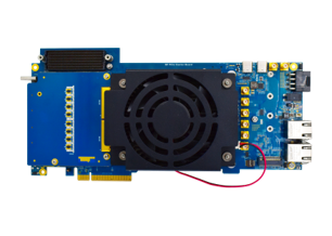
  • Agilex™ 9 AGRW014 Direct RF SOM Development Platform
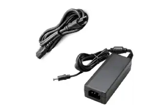
  • 12V, 5A Power Supply
  • Safety guidelines
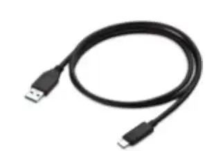
  • USB Debug cable
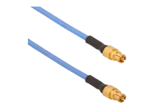
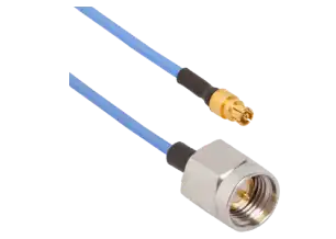
  • SMPM to SMPM Cables
  • SMPM to SMA cables
Agilex 9 AGRW014 SOM Development Platform

Agilex™ 9 AGRW014 SOM Development Platform

12V, 5A Power Supply

12V, 5A Power Supply 

USB Debug cable

USB Debug Cable

SMPM to SMPM cable

SMPM to SMPM cable

SMPM to SMA cable

SMPM to SMA cable

Safety Guidelines

Environmental Compliance
iG-G67P Agilex™ 9 AGRW014 Direct RF FPGA SoC based SoM Development platform is designed by using RoHS and REACH compliant components and manufactured on lead-free production process.

Environmental Compliance

ESD Protection
This development platform is ESD sensitive. Handle the product only in accordance with the installation instructions given in the manual. Therefore, ESD precautions should be taken care during transport and handling. Must use a ESD ground strap or other grounded source before unpacking or handling the hardware.

ESD Protection

Product Disposal
Check the local regulations for disposal of electronic products before disposing.

Product Disposal

Get to know

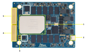
Agilex 9 AGRW014 Direct RF SOM – Top view

Agilex™ 9 AGRW014 Direct RF SOM – Top view

  1. Agilex 9 AGRW014 Direct RF FPGA
  2. Fan Header
  3. Switch

4. RF – GPPC connector 1 (DAC)
5. RF – GPPC connector 2 (ADC)

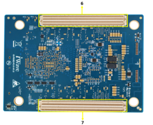
Agilex 9 AGRW014 Direct RF SOM Bottom view

Agilex™ 9 AGRW014 Direct RF SOM – Bottom view

  1. Board to Board connector 2
  2. Board to Board connector 1
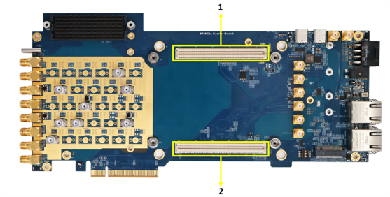
Agilex 9 AGRW014 Direct RF Development Platform – Top view-1

Agilex™ 9 AGRW014 Direct RF Development Platform – Top view-1

  1. Board to Board Connector 1
  2. Board to Board Connector 2
Agilex 9 AGRW014 Direct RF Development Platform Top view 2

Agilex™ 9 AGRW014 Direct RF Development Platform – Top view-2

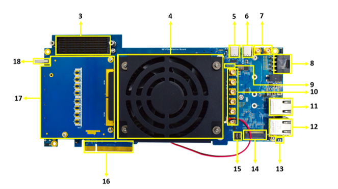
  1. FMC+ Connector
  2. Agilex 9 SOM FanSink
  3. Type-C Connector
  4. Type-C DP**
  5. SMA Connector
  6. Power Connector
  7. JTAG Connector
  8. SMA connectors clock input

11. RJ45 Magjack Connector – 1
12. RJ45 Magjack Connector – 2**
13. Reset Switch.
14. M.2 KEY M connector.**
15. Boot Media SEL Switch
16. PCIe x16 Connector
17. RF Daughterboard.
18. Type C Debug.

Agilex 9 AGRW014 Direct RF Development Platform Bottom view

Agilex™ 9 AGRW014 Direct RF Development Platform – Bottom view

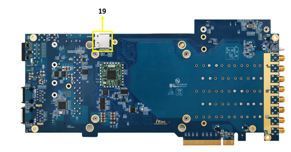
  1. Micro SD connector *

*Optional

**Not Supported

Note: RF is supported through iWave’s RF BALUN daughterboard.

Download FTP Contents

All the technical resources of iG-G67P Agilex™ 9 AGRW014 Direct RF FPGA SoC based SoM  Development platform is available in iWave FTP server.

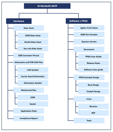
FTP Folder Structure

FTP Folder Structure

For FTP Credentials, Contact : mktg@iwave-global.com

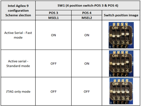
Boot Switch Setting

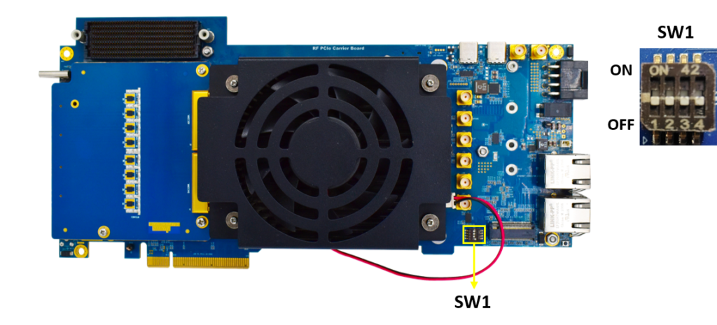
Make sure On-Board Switch (SW1) is set properly as shown below image

Boot Switch Setting

SW 1-Boot Selection Switch

Configuration Selection Truth Table


Configuration Selection Truth Table

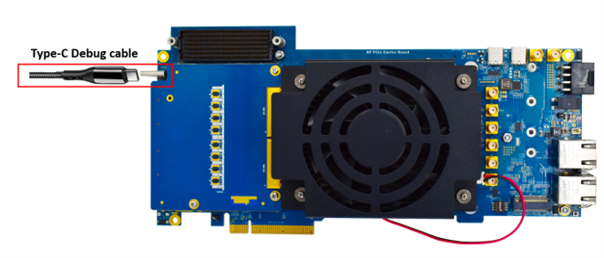
Debug Port Setting

Connect Type-A end of USB cable to PC and Type-C end of USB cable to

Development platform’s debug Type C connector(J7) as shown below.

Debug Port Setting
  • Setup the Debug Terminal parameters.
  • Baud Rate : 115200
  • Data bits : 8
  • Parity : None
  • Stop Bits : 1
  • Flow Control: None

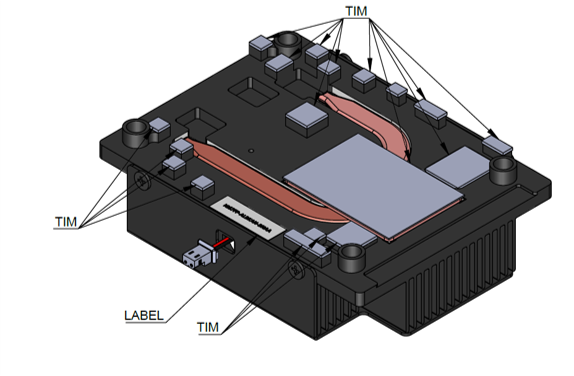
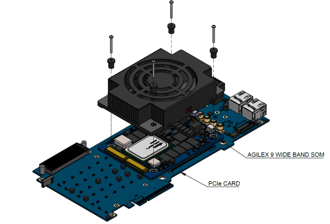
Fan sink Connection

Before mounting the heat sink and fan assembly, remove the protective cover attached to the top of the TIM (Thermal Interface Material).

Fan sink Connection

Mount the screws following the instructions shown in the image below.

Mount the screws PCIe card

How to configure

Minicom
Tera Term
Putty

On the command prompt of the Linux host machine, run the following command to determine the port number:
$ ls /dev/ttyUSB*

Minicom

Use the following commands to install and run the serial communication program (minicom as an example):

  • Install Minicom using Ubuntu package manager.
         $ sudo apt-get install minicom
  • Launch Minicom using a console window using the port number determined earlier.
         $ sudo minicom -D /dev/ttyUSB1
  • Configure Minicom as show in below figure
Minicom Window

Next step is to Power ON the board.

Install the driver for Debug USB Port in Host PC/Laptop using the below link.
http://ftdichip.com/drivers/vcp-drivers/

  • Download Tera Term and install it.
    • Launch Tera Term and power ON the board.
      Select the serial option. After your board is plugged in, there should be a COM port automatically populated in the list.
Tera Term connection window
  • Configure the Serial Port Settings.

   Go to Setup – Serial Port and change the settings as shown below.

Tera Term port window
  • Verify the title bar in Tera Term to confirm that the connection is established correctly.
Tera Term Com window
  • Next step is to Power ON the board.

Install the driver for Debug USB Port in Host PC/Laptop using the below link.
http://ftdichip.com/drivers/vcp-drivers/

  • Download PuTTY and install the application. webpage to continue.
  • Launch PuTTY 
  • Power ON the board
    Enter the appropriate COM port and configure the speed (baudrate) to 115200
Putty window
  • Click “Open” to open the serial connection.
  • Next step is to Power ON the board.

Powering ON

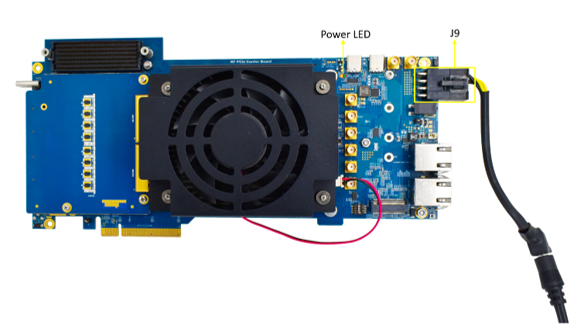
Connect the Power supply plug to the Power connector (J9) of the Development platform as shown below and switch ON the power supply. Once power is applied to the Development platform, the power LED in the Development platform will glow as shown in the below image.

Powering ON

Warning:

Test Environment setup

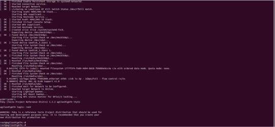
Once power is applied to the Development Platform as explained in the previous section, boot messages being displayed in the debug terminal of the PC/Laptop which is connected to the Development platform. Press any key in terminal immediately to see the command prompt of the Boot loader or wait until OS boots. After OS boots, Login prompt being displayed in the debug terminal. Enter username and password as “root” to get the Linux command prompt as shown below.

Test Environment setup


JTAG Connection

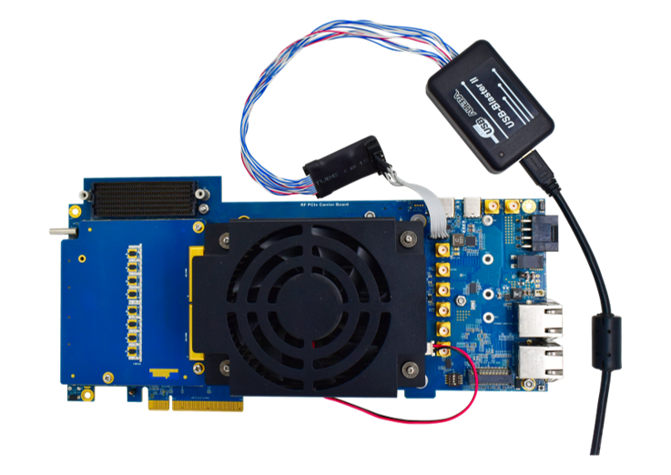
iG-G67P Agilex™ 9 AGRW014 Direct RF FPGA SoC based SoM PCIe Development platform support JTAG interface for FPGA Programming and debugging. Use the USB Blaster to connect Carrier Board. Ensure that Switch-1 on the carrier board is turned OFF.

Example USB Blaster which is tested with this Platform is mentioned below.
USB Blaster-2
Part Number :  PL-USB2-BLASTER from Altera

JTAG Connection
img
Click outside to hide the comparison bar
Compare
Compare ×
Let's Compare! Continue shopping