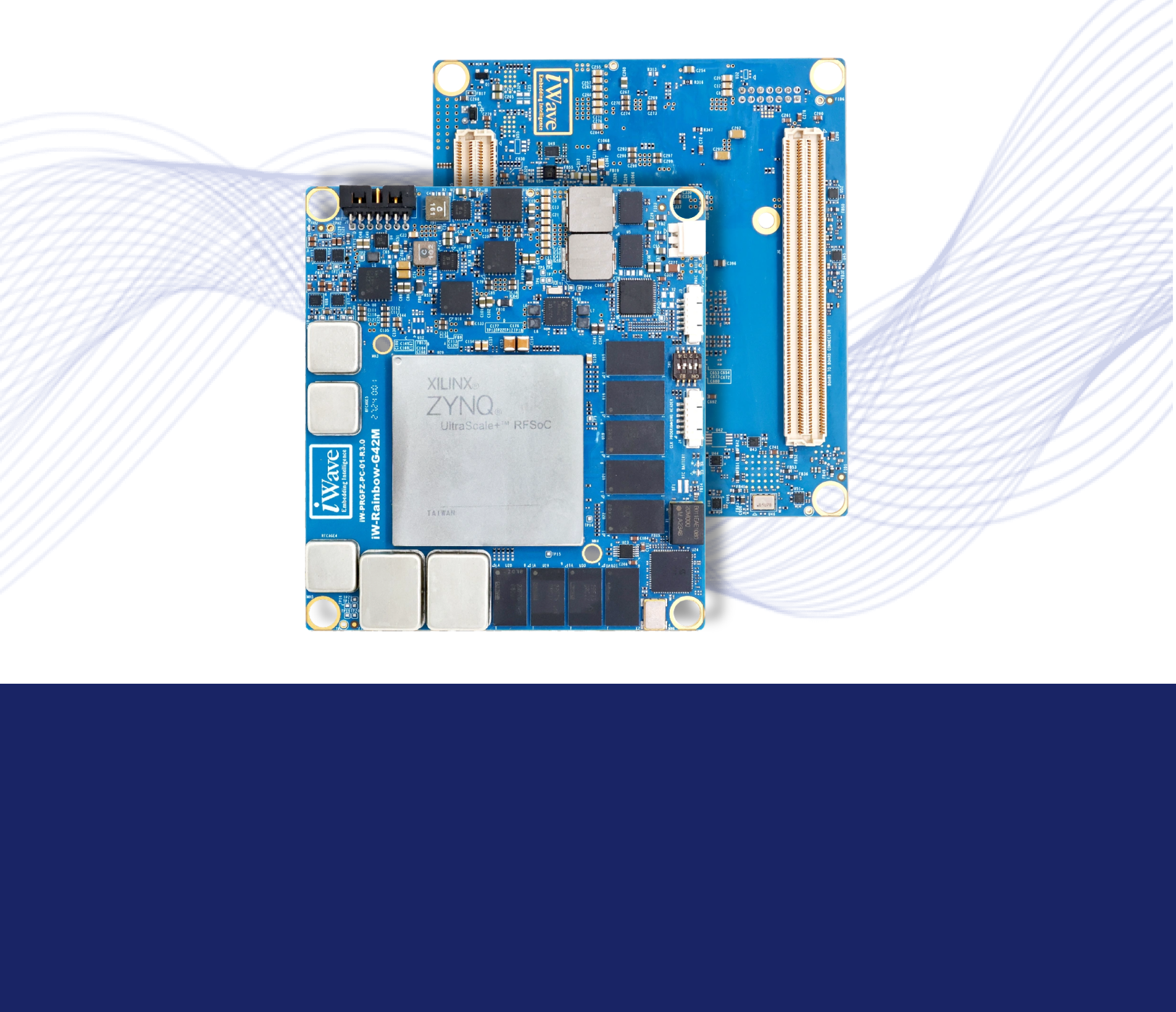
| Zynq Ultrascale+ RFSoC ZU67/65/64/63DR |
Processing System (PS)
- Quad-core ARM Cortex-A53 MPCore Application processor (up to 1.3GHz)
- Dual-core ARM Cortex-R5 MPCore Real Time Processor (up to 600MHz)
Programming Logic (PL)
- Programming Logic (PL) with up to 489K Logic cells
- PL GTY High Speed Transceivers x8 @ up to 28.21 Gbps
|
| RAM Memory |
- 64bit, 8GB DDR4 RAM for PS with ECC
- 32bit, 4GB DDR4 RAM for PL
|
| Flash Memory |
- 256MB QSPI Flash for Booting
- 32GB eMMC Flash for Storage
- 2-Kbit EEPROM x2
|
| Clock & PLL |
- Integrated Configurable ultra-low noise PLL for ADC & DAC
- Fully Configurable Clock Synthesizer with SyncE and PTP support
|
| 3U VPX Backplane Features
3U VPX Connector – P0+P1A |
Data Plane Port: DP01[3:0]
- 100GbE/40GbE KR4 using PL GTY Bank Transceivers
Data Plane 1 Ultra-Thin Pipe
- DPutp01 – LVDS pair x2 or single ended I/Os x4 (Optionally supports 10GBASE-KR using PL GTY Bank Transceivers)
Control Plane Ultra-Thin Pipe
- CPutp01 – LVDS pair x2 or single ended I/Os x4 (Optionally supports 10GBASE-KR using PL GTY Bank Transceivers)
System and Power Signals
- System Control Signals
- System Reference and Auxiliary Clocks
- Bussed GPIO
- Maintenance Port (MP01)
- Power Input (12V (Vs1), 3.3V AUX, VBAT)
|
| 3U VPX Backplane Features
3U VPX Connector (P1B+P2A) |
Expansion Port
- LVDS pair x14 or single ended I/Os x28
|
| NanoRF +MT Ferrule Hybrid Connector -(P2B) |
- 4 RF ADC inputs, configurable from 30 MHz to 6 GHz, with sampling rates up to 5 GSPS
- 4 RF DAC outputs, configurable from 30 MHz to 6 GHz, with sampling rates up to 2.95 GSPS
- Hybrid optical MT Ferrule using PL GTY Bank Transceivers, supporting up to 100GbE/40GbE
- External trigger input
- External reference clock input
|
| Front Panel Features |
- SMPM male connectors ×8 (2 RF ADC channels with sampling rates up to 2.95 GSPS, 2 RF ADC channels with sampling rates up to 5.9 GSPS, and 4 RF DAC channels with sampling rates up to 10 GSPS)
- USB 3.0/2.0 Type-C Connector
- 10/100/1000 Mbps Ethernet 9-pin Header
- 3-pin Debug UART Header
- Micro-SD Connector
|
| On-Board Features |
- PCIe Gen2 x2 through M.2 Connector
- Temperature Sensor
- Elapse Time Counter
- Clock Synthesizer for Transceiver Reference clocks
|
| General Specification |
- Power Input: +12V (Vs1) and 3V3_AUX input from VPX Connector
- Thermal Solution: Integrated Heat Spreader
- Form Factor: 3U VPX (160mm X 100mm)
- Module Profile: MOD3p-PAY-1F1U1S1S1U1U4F1J-16.6.13-n
- Slot Profile: SLT3p-PAY-1F1U1S1S1U1U4F1J-14.6.13-n
- Also Supports other SLT3 slot profiles
- Slot Pitch: 1 Inch Conduction Cooled
- Operating Temperature: -40°C to +85°C (Industrial)
- Environment Specification: REACH & RoHS Compliant
|